- 您现在的位置:买卖IC网 > Sheet目录1217 > GDBD4410 (IXYS)BOARD EVALUATION IXBD4410/11
�� �
�
�GDBD� 4410�
�Power� Supply�
�One� power� supply� with� a� single,� ground�
�referenced� voltage� V� DD� is� required� for� all�
�four� low� side� drivers� within� the� driver� unit�
�together.� It� shall� be� connected� between�
�the� terminals� +2467� (plus)� and� M2467�
�(ground).�
�The� high� side� drivers� for� transistors� T1,� T3�
�and� T5� can� be� supplied� in� one� of� the�
�following� ways:�
�?� power� supplies� on� separate� potentials�
�-� Those� typically� make� use� of� additional�
�secondary� windings� of� the� transformer�
�which� is� used� in� an� existing� auxiliary�
�switched� mode� power� supply� anyway.�
�However� only� one� output� voltage� can� be�
�controlled� in� this� case.�
�-� Alternatively,� DC-DC� converters� with� high�
�insulation� voltage� might� be� used.�
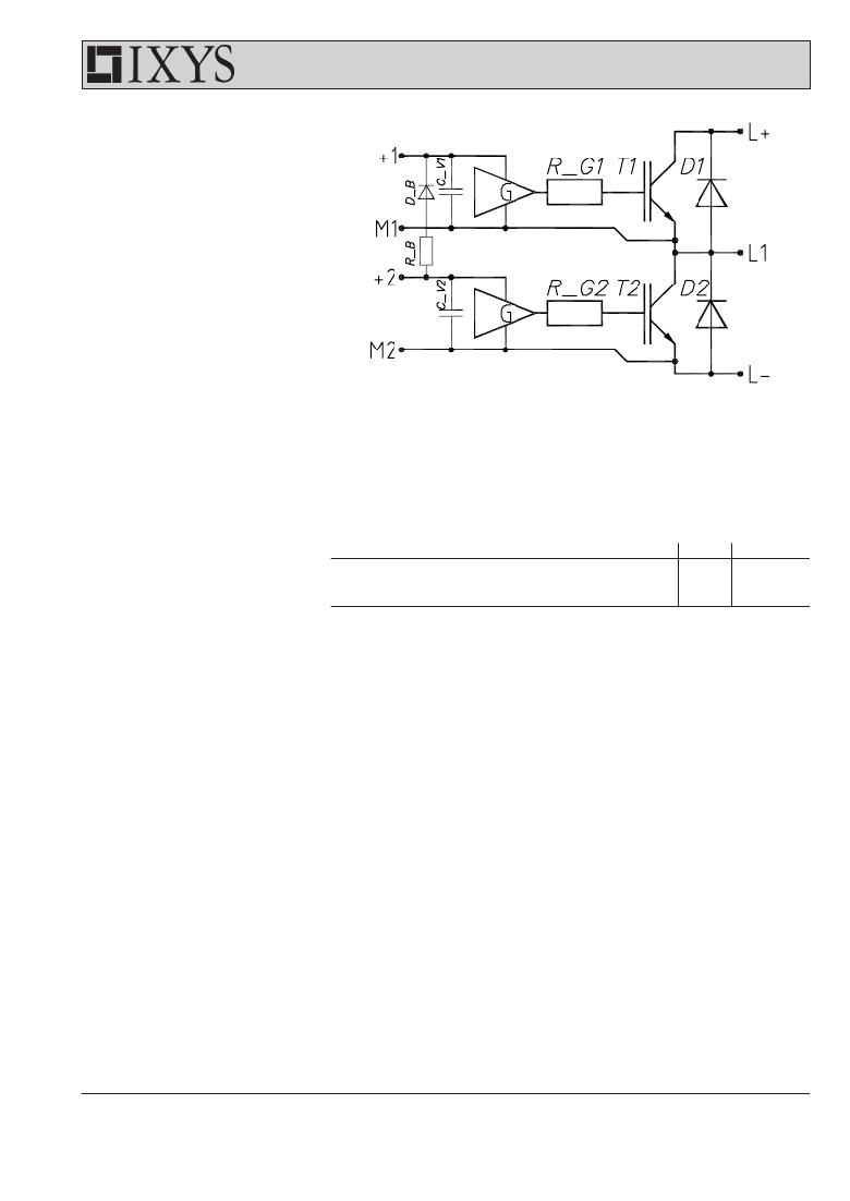
�?� bootstrap� circuit�
�The� circuit� is� exemplary� shown� for� a� phase-�
�leg� in� figure� 2:�
�-� When� low� side� transistor� T2� or� diode� D2� is�
�conducting,� high� side� ground� M1� is� on�
�potential� of� low� side� ground� M2� plus�
�saturation� voltage� U� CEsat� of� T2� or� minus�
�Fig.� 2� Bootstrap� circuit�
�forward� voltage� U� F� of� D2.� Plus� of� low� side�
�driver� supply� +2� thus� can� charge� the� buffer�
�capacitor� for� the� high� side� driver� supply�
�Symbol�
�Definitions/Conditions�
�Characteristic� Values�
�(T� VJ� =� 25°C,� V� DD� =� 15� V� unless� otherwise� specified)�
�min.� typ.�
�max.�
�C� V1� via� high� voltage� diode� D� B� and� current�
�limiting� resistor� R� B� .�
�Quiescent� Power� Supply� Current�
�-� When� low� side� transistor� T2� and� diode� D2�
�are� off,� high� side� transistor� T1� can� be� driven�
�I� DD�
�V� DD� Current/V� in� =� V� DD� or� LG,� I� D� =� 0�
�20�
�mA�
�with� the� charge� stored� in� C� V1� .� When� T1� or�
�D1� are� conducting,� bootstrap� diode� is�
�blocking� about� DC� link� voltage.�
�It� should� thus� be� noted� that�
�-� regular� turn� on� of� T2� or� D2� is� mandatory� for�
�operation� of� this� circuit,� otherwise� there� is�
�no� supply� for� T1� driver�
�-� T1� driver� supply� voltage� level� is� quite�
�inaccurate,� also� depending� on� T2� U� CEsat� or�
�D2� U� F� respectively�
�-� bootstrap� diode� D� B� has� to� be� rated� for�
�operation� with� DC� link� voltage�
�-� bootstrap� resistor� R� B� should� be� sized� in� a�
�way� that� charging� of� C� V1� is� effectuated�
�within� the� minimum� on� time� of� T2� or� D2�
�respectively�
�-� bootstrap� diode� D� B� and� resistor� R� B� have� to�
�sustain� the� charging� current� peaks.�
�Bootstrap� circuits� for� the� three� high� side� drivers�
�can� easily� be� placed� on� the� printed� circuit�
�board,� the� driver� unit� is� connected� to,� between�
�pins� +2467� and� +1� or� +3� or� +5� respectively.�
�Generally,� supply� voltage� levels� of� V� DD� =� 15�
�V� are� recommended.�
�?� 2004� IXYS� All� rights� reserved�
�5-6�
�发布紧急采购,3分钟左右您将得到回复。
相关PDF资料
GH1250
FUSE INDUST 1250A 550V 84X198MM
GMF.3K.085.EANZ
RUBBER BOOT
GPIODM-KPLCD
BOARD DEMO LCD GPIO EXP KEYPAD
GSAP 15-R
FUSE 15A 250VAC AXIAL SLOW
GSB3211311WEU
USB 3.0 DIP B RECP THRU HOLE
GSB343K33HR
USB 3.0 MICRO B RECP SMT
GT-BG230L
ARRESTOR 230VDC HD GASTUBE GLASS
GT-BG350L
ARRESTOR 350VDC HD GASTUBE GLASS
相关代理商/技术参数
GDBE111630-19
制造商:ITT Interconnect Solutions 功能描述:GDBE111630-19 - Bulk
GDBE-25S-A156
制造商:ITT Interconnect Solutions 功能描述:GDBE-25S-A156 - Bulk
GDB-V-1.25A
制造商:Cooper Bussmann 功能描述:Fuse Miniature 1.25A 250V Fast 2-Pin Axial Through Hole Cardboard Carton
GDB-V-1.6A
制造商:Cooper Bussmann 功能描述:
GDB-V-100MA
制造商:Cooper Bussmann 功能描述:
GDB-V-10A
制造商:Cooper Bussmann 功能描述:
GDB-V-125MA
制造商:Cooper Bussmann 功能描述:Fuse Miniature 0.125A 250V Fast 2-Pin Axial Through Hole Cardboard Carton
GDB-V-160MA
制造商:Cooper Bussmann 功能描述:Fuse Miniature 0.16A 250V Fast 2-Pin Axial Through Hole Cardboard Carton